
The Ultra-Thin Metasurface Chip, developed by Harvard physicists, marks a major breakthrough in quantum optics. By collapsing complex optical systems onto a chip just nanometers thick, it paves the way for compact, next-gen quantum processors with military and communication applications, triggering a global race in quantum technology innovation.
KumDi.com
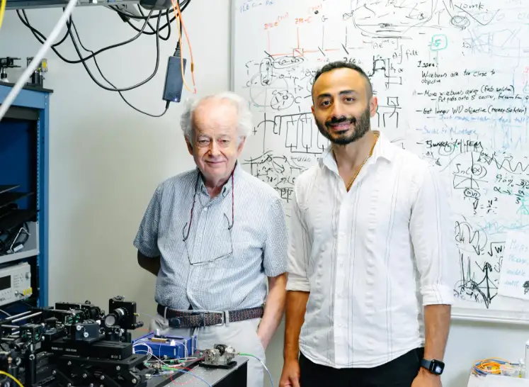
Harvard researchers have created an ultra-thin metasurface quantum chip capable of collapsing entire quantum-optical setups into a single flat device. Led by top scientists in quantum optics, the chip uses graph-theory-based nanoscale design to entangle photons and perform quantum operations at room temperature. This innovation dramatically enhances scalability, stability, and field deployment potential—ushering in a new era of quantum optics and advanced military applications.
Table of Contents
What is the Ultra-Thin Metasurface Quantum Chip?
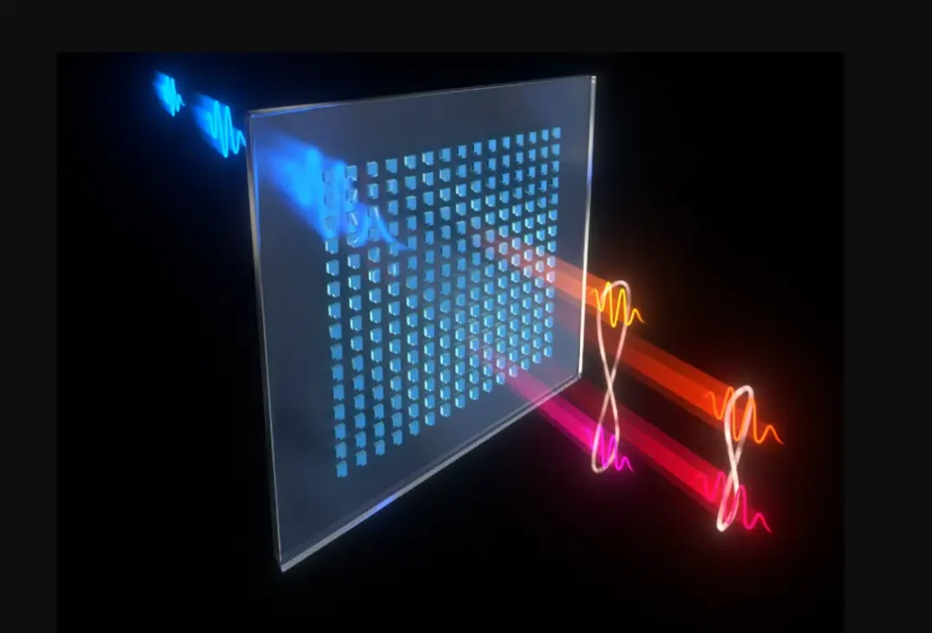
The chip is built from a nanostructured surface that mimics the function of waveguides, beam splitters, and lenses—all within a thin photonic platform. This metasurface can manipulate single photons to form entangled quantum states, enabling quantum computing and communication on a compact scale. Unlike traditional quantum systems, it operates at room temperature, making it highly adaptable for real-world use cases, especially in defense and aerospace.
Why This Matters for Military and Tech Industries
Scalability and Miniaturization
This chip replaces bulky quantum optics setups with a single, flat, scalable layer. Its compactness enables integration into drones, satellites, and mobile defense units.
Room-Temperature Quantum Operations
The chip supports quantum functions without the need for cryogenics, significantly reducing energy needs and improving system portability and maintenance.
Strategic Military Advantage
Defense agencies are interested in the chip’s potential to power unhackable communication systems, advanced quantum radar, and autonomous navigation powered by quantum AI.
How It Works: Graph Theory Meets Nanophotonics
The design leverages graph theory to precisely map photon paths and interactions into a physical surface pattern. These etched nanoscale features control how photons move, interact, and become entangled—all on a single chip. This approach collapses the entire optical quantum system into a reliable, compact platform, eliminating common sources of interference and instability.
Global Race Triggered by Breakthrough
With the announcement of this technology, a new wave of funding and defense interest has swept across the United States, China, and Europe. Government agencies and private contractors are racing to scale, adapt, and militarize the technology to gain strategic dominance in the emerging quantum battlefield. This innovation is expected to reshape both civilian and defense sectors over the coming decade.
Challenges and Future Directions
While promising, the chip faces challenges in scaling to handle more complex photon entanglement networks. Mass production and long-term coherence over time and in diverse environments are also areas of ongoing research. Nonetheless, this development represents a foundational step toward practical, portable quantum systems.
FAQs
What is the ultra-thin metasurface quantum chip by Harvard?
It is a nanoscale chip that combines the functions of optical components into a flat surface, enabling quantum photon manipulation and entanglement in a compact format.
How does the metasurface chip simplify quantum optics?
It replaces traditional bulk optics by integrating photon routing and entanglement into a single surface, enhancing stability and miniaturization.
Who developed this metasurface quantum chip?
Harvard scientists specializing in quantum optics and nanophotonics engineered the chip using graph-theory-based nanostructure design.
Why is this chip significant for military applications?
It enables portable, secure quantum systems for defense, including stealth detection, quantum radar, encrypted communication, and autonomous battlefield intelligence.
What are the challenges with metasurface quantum chips?
Scaling complexity, maintaining quantum coherence, and achieving high-yield manufacturing remain the primary hurdles before full deployment.


